Can the contact mechanism between SIM card's gold fingers and card socket inspire neural synaptic connections in micro-robots?
- Share
- publisher
- Moarconn
- Issue Time
- May 6,2025
Summary
Let's dive into the microscopic universe of SIM cards, dissecting every detail from the plastic frame to nano-scale connections, and unveil the engineering marvel behind dual-SIM trays.
Got it! Let's dive into the microscopic universe of SIM cards, dissecting every detail from the plastic frame to nano-scale connections, and unveil the engineering marvel behind dual-SIM trays. Magnifying glass ready? Let's get started!
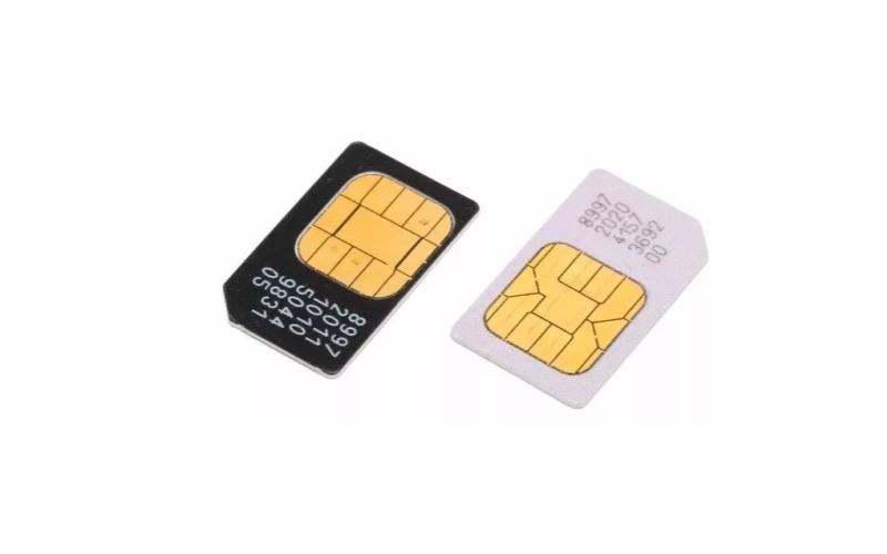
I. Physical Anatomy of a SIM Card
1. Chip Architecture: Secrets Beneath the Gold Fingers
Gold-plated contacts: 6-8 copper pads (typically 6), each assigned a specific role per ISO 7816 standards:
C1 (VCC): Power input (1.8V/3V/5V adaptive)
C2 (RST): Reset signal
C3 (CLK): Clock signal (1-5MHz)
C5 (GND): Ground
C6 (VPP): Programming voltage (mostly obsolete)
C7 (I/O): Data channel
2. Nano-Scale Manufacturing
Thickness: 0.12mm—thinner than an A4 sheet!
Wafer material: Silicon dioxide substrate + copper alloy circuits
Encapsulation: COB (Chip on Board) process with epoxy resin sealing
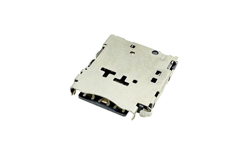
II. Nano SIM Socket: Micron-Level Precision
1. Mechanical Design
plaintext
┌─────────────────┐
│ Spring-loaded pins │← Contacts SIM gold fingers
├─────────────────┤
│ Guide rails │← Ensures insertion orientation
├─────────────────┤
│ Self-locking latch │← Source of the "click" sound
└─────────────────┘
2. Contact Engineering
Spring force: 50-100gf per pin
Durability: 0.2μm gold plating withstands 5,000 insertions
Anti-misinsertion: Beveled edges + asymmetric notches
3. Electrical Specifications
| Parameter | Requirement | Testing Method |
|-----------------|----------------------|----------------------|
| Contact Resistance | <100mΩ | Four-wire measurement |
| Insulation Resistance | >100MΩ (500VDC) | Hi-pot tester |
| Operating Temp | -25℃~+85℃ | Thermal cycling |


III. Dual-SIM Tray Design: Space Optimization Masterclass
1. Main Dual-SIM Architectures
| Type | Structure | Example Devices |
|------------------|-------------------------------|----------------------|
| Stacked | Vertical layers sharing space | Huawei P30 |
| Parallel | Side-by-side slots | Xiaomi 10 |
| Flip-Flop | Double-sided design | iPhone XR (US model) |
2. Material Evolution
Gen 1: Stainless steel (prone to bending)
Gen 2: Titanium alloy + CNC machining (since iPhone 6)
Cutting-edge: Liquidmetal (Zr-based amorphous alloy), 3x stronger!
3. Mechanical Engineering
Insertion force: 1.5-2.5N (fingernail pressure)
Ejection mechanism: Spring + inclined plane leverage
IV.Extreme Environment Testing
Military-Grade SIMs
Temperature: -40℃~+105℃ (vs. -25℃~+85℃)
Shock resistance: 50G impact (10m drop equivalent)
Waterproofing: IP68-rated, survives 72hr submersion
V. Repair Technician's Guide
1. Troubleshooting
| Symptom | Cause | Solution |
|---------------------|---------------------------|-----------------------|
| "No SIM" error | Oxidized contacts | Clean with eraser |
| Intermittent signal | Worn socket springs | Replace socket |
| Undetected SIM | Voltage mismatch | Adjust via AT commands|
2. DIY Risks
Manual cutting: Risk of micro-cracks (requires microscope)
Hot air soldering: >260℃ damages chip
Jumper recovery: Only feasible on C6/C7 pins
Who knew a tiny SIM card hides a universe of engineering marvels? From nano-scale contacts to space-ready designs, every detail safeguards your digital identity. Next time you hold a SIM, admire those golden traces—they’re your gateway to the connected world! ✨
Want deeper dives? Need a cross-sectional diagram of the socket or microscope images of SIM circuits? Just ask! 😄