PCB Footprint & Layout Best Practices for SD Card Connectors
- Share
- publisher
- MOARCONN
- Issue Time
- Sep 16,2025
Summary
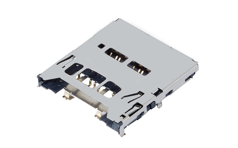
At Moarconn (www.moarconn.com), we specialize in SIM, SD, microSD, and Nano SIM card connectors that combine durability, precision, and performance.
Introduction
SD card connectors are critical components in modern electronic devices, enabling reliable data storage and transfer in applications ranging from consumer electronics to industrial systems. However, their performance largely depends on proper PCB footprint design and layout practices. Without careful attention to details such as signal integrity, grounding, and mechanical support, engineers may face issues like poor contact, EMI noise, or long-term durability problems.
At Moarconn, a professional manufacturer of card connectors including SIM, microSD, and SD card connectors, we help engineers overcome these challenges by providing high-quality, durable solutions optimized for real-world applications.
Key Considerations for PCB Footprint Design
Pad Dimensions and Tolerances
Accurate pad design is fundamental. Pads must align precisely with connector pins to ensure consistent solder joints. Following IPC standards for pad size and spacing reduces the risk of bridging or cold solder joints.
Solder Mask and Paste Apertures
A well-defined solder mask opening prevents solder bridging between adjacent pins. For fine-pitch SD card connectors, optimized paste apertures improve solder joint reliability during reflow.
Mechanical Support and Reinforcement
Since SD cards are removable, connectors endure repeated insertions and withdrawals. To ensure mechanical robustness, use non-plated holes or anchor pads for reinforcement. This prevents stress on solder joints and extends product lifecycle.

Layout Best Practices for SD Card Connectors
Signal Integrity and Trace Routing
High-speed interfaces such as SD Express require controlled impedance routing. Keep traces short, avoid unnecessary vias, and maintain consistent differential pair spacing for high-speed signals.
Grounding and EMI Shielding
Placing ground vias near the connector improves shielding and reduces EMI. A solid ground plane beneath the connector footprint further enhances signal stability.
Clearance and Accessibility
Leave adequate clearance around the connector to allow easy insertion and removal of the SD card. Consider end-user ergonomics, especially for handheld or compact devices.
Common Mistakes to Avoid
Misaligned pad dimensions leading to poor solderability
Ignoring mechanical reinforcement, causing connector damage over time
Excessive via usage near signal pads, degrading high-speed performance
Lack of ground shielding, leading to EMI interference
Why Choose Moarconn for SD Card Connectors
At Moarconn (www.moarconn.com), we specialize in SIM, SD, microSD, and Nano SIM card connectors that combine durability, precision, and performance. Our connectors are widely used in industrial IoT, consumer electronics, and automotive applications. With strict quality control and customizable design support, we help engineers integrate card connectors seamlessly into their PCB designs.
Conclusion
Designing the PCB footprint and layout for SD card connectors is a detail-oriented process that directly impacts product reliability and performance. By following best practices—such as proper pad sizing, EMI shielding, and reinforcement—engineers can minimize risks and extend product lifecycle.
With Moarconn’s high-quality SD card connectors, you gain the advantage of reliable components designed for long-term durability and precision. Visit www.moarconn.com to explore our range of card connector solutions and get expert support for your next project.