SD Card Connectors: DFM & PCB Footprint Guide by Moarconn
- Share
- publisher
- MOARCONN
- Issue Time
- Nov 26,2025
Summary
DFM-focused guide for SD card connectors with PCB footprint tips, layout best practices, and reliable connector solutions from Moarconn.


Introduction
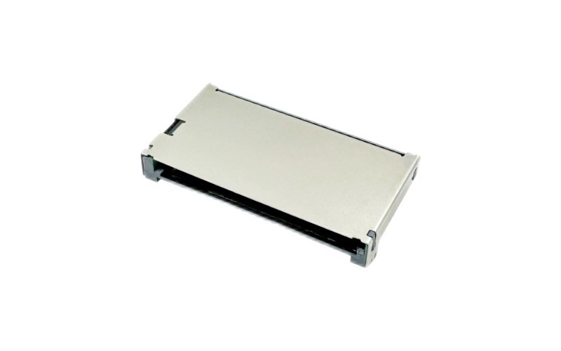
SD card connectors are widely used in consumer electronics, industrial devices, IoT products, and embedded systems. But creating a reliable PCB footprint for an SD or microSD connector requires much more than simply drawing pads. A poorly designed footprint may cause soldering failures, weak joints, EMI problems, or long-term reliability issues.
At Moarconn (www.moarconn.com), we specialize in SD, microSD, SIM and Nano SIM connectors. With years of manufacturing and SMT experience, we understand the engineering challenges behind connector design. This guide provides DFM (Design for Manufacturability) best practices, PCB footprint rules, and practical advice to help engineers design robust products.
Why DFM Matters
A DFM-optimized SD card connector footprint helps ensure:
High soldering yield and consistent SMT assembly
Strong mechanical durability during repeated insertions
Better signal integrity at higher data rates (UHS-I / UHS-II / SD Express)
Long-term product reliability in real-world usage
1. Pad Geometry & Solder Mask
Follow the connector datasheet strictly. Small deviations in pad width, pitch, or solder mask opening can lead to solder bridging or misalignment. For fine-pitch connectors, NSMD pads usually provide better solder fillets and joint reliability.
2. Mechanical Reinforcement
Use mechanical anchors, shell solder points, or NPTH holes for stability. This prevents solder joint cracking or pad lifting, especially in devices with frequent card insertion/removal.
3. Grounding, EMI & Signal Integrity
Keep data/clock traces short and provide solid grounding paths. Avoid vias under pads to prevent solder wicking. Add stitching vias around the connector shell for EMI shielding.
4. Component Placement & Clearance
Place the connector near the PCB edge to allow smooth card insertion. Keep heat sources, high-frequency ICs, and sensitive analog circuits away from the slot.
Common Mistakes to Avoid
Pads are too small or solder mask is misaligned → weak joints
No mechanical anchoring → shell becomes loose
Long trace routing → EMI & signal errors
Vias under pads → solder wicking or poor reflow
No clearance zone → card cannot fully insert
Why Choose Moarconn
Moarconn offers:
Precision SD & microSD connector manufacturing
LCP high-temperature housings
Gold-plated terminals with excellent durability
Customizable footprints, metal shells, or ejector designs
Strict QC testing: insertion/withdrawal, vibration, thermal cycling
Workflow for Engineers
Review connector datasheet carefully
Create footprint based on recommended pads
Plan grounding & high-speed routing strategy
Add mechanical anchors and keep-out areas
Validate insertion space & enclosure clearance
Perform reflow, assembly and insertion tests
Conclusion
By following DFM rules and PCB footprint best practices, engineers can significantly improve assembly yield, long-term reliability, and overall product stability. Combined with Moarconn’s high-quality SD card connectors, your device can achieve industry-leading durability and performance.