Nano SIM Card Connector PCB Footprint and SMT Design Guide
- Share
- publisher
- MOARCONN
- Issue Time
- Oct 13,2026
Summary
Learn Nano SIM Card Connector PCB footprint design, SMT assembly, soldering tips, and verification for reliable electronics.
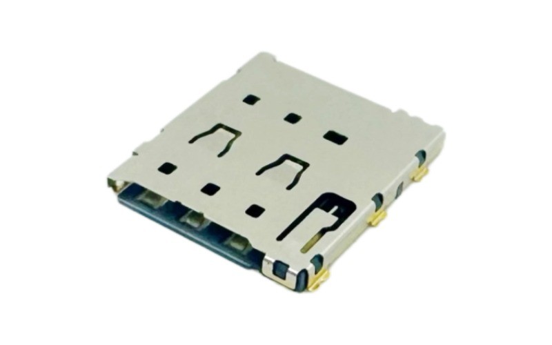
Nano SIM Card Connector PCB Footprint and SMT Design Guide
Designing a reliable Nano SIM Card Connector footprint involves more than placing solder pads on a PCB. Engineers must verify the manufacturer's land pattern, check mechanical clearances, understand the contact layout, plan the surface-mount technology (SMT) process, and validate the assembled connector under real operating conditions.
A small footprint error can lead to poor solder joints, mechanical interference, inconsistent card contact, or costly PCB redesigns. These risks become more important in compact IoT devices, cellular gateways, industrial electronics, wearables, and other space-constrained products.
In this Engineer's Notebook guide, Moarconn explains how to approach Nano SIM connector PCB footprint design, SMT assembly planning, and pre-production verification. The goal is to help hardware engineers reduce avoidable design errors and make more informed connector decisions before committing to mass production.
Quick takeaway: Always start with the latest datasheet and recommended PCB land pattern for the exact connector part number. Then verify the footprint against the mechanical drawing, assembly process, and final product enclosure.
1. Understanding a Nano SIM Card Connector PCB Footprint
A PCB footprint defines the physical land pattern and component placement information needed to mount an electronic component onto a printed circuit board.
For a Nano SIM Card Connector, the footprint must accommodate the electrical contacts, mounting or grounding terminals, mechanical locating features where applicable, and the connector's overall physical envelope.
It must also work with the card insertion mechanism and the surrounding enclosure.
1.1 Nano SIM Card Dimensions vs. Connector Dimensions
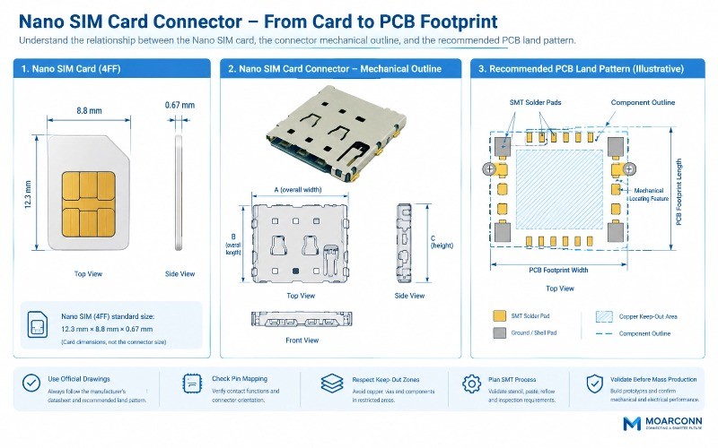
A standard Nano SIM card uses the 4FF form factor, with nominal dimensions of 12.3 mm × 8.8 mm × 0.67 mm.
These dimensions describe the card, not the connector or its PCB footprint.
The connector's overall dimensions depend on its design, including the mounting style, card retention mechanism, profile height, contact arrangement, and housing structure.
For example, a compact push-pull connector and a hinged Nano SIM connector may accept the same card format but require different PCB land patterns and mechanical clearances.
Before starting the PCB layout, confirm the following:
The exact connector manufacturer and part number.
The connector's recommended PCB land pattern.
The contact numbering and electrical pin assignments.
The connector height and overall mechanical dimensions.
The card insertion direction and required access space.
Any mounting holes, locating features, or copper restrictions.
Engineering note: Never create a Nano SIM connector footprint by scaling a product photograph or copying the footprint of a visually similar component. Even connectors designed for the same card format can have different pad locations and mechanical requirements.
1.2 What Is Included in a Recommended PCB Land Pattern?
Depending on the connector design, the recommended land pattern may include:
SMT solder pads for electrical contacts.
Ground or shell solder pads.
Mechanical mounting pads or locating features.
Component outline and placement reference.
Areas restricted for copper, vias, or other components.
Dimensional tolerances and PCB manufacturing notes.
The exact features vary by model. Use the manufacturer's drawing rather than assuming that every Nano SIM connector has the same pad arrangement.
2. How to Read a Nano SIM Connector Datasheet
A connector datasheet is the primary reference for footprint creation and PCB integration. Before routing traces or preparing the SMT assembly files, review the mechanical drawing, recommended PCB layout, pin connections, and applicable assembly instructions.
2.1 Check the Recommended PCB Layout
Look for a drawing specifically labeled "Recommended PCB Layout," "PCB Footprint," or "Recommended Land Pattern."
Confirm whether the drawing shows a top view or a bottom view. A mirrored footprint or incorrect connector orientation can reverse the intended pin mapping.
Check the following details:
Pad dimensions and spacing.
Contact pitch and pad positions.
Overall component outline.
Mechanical locating features.
Ground and shell connection locations.
Copper-restricted or component keep-out areas.
PCB tolerance requirements.
Use the stated units and tolerances. Do not assume that dimensions are in millimeters unless the drawing confirms this.
2.2 Verify Pin Numbering and Electrical Functions
A typical six-contact SIM interface uses the following contact functions:
| SIM Contact | Typical Function |
| C1 | VCC — supply voltage |
C2 | RST — reset |
C3 | CLK — clock |
C5 | GND — ground |
C6 | VPP — programming voltage, where applicable |
C7 | I/O — data |
The exact implementation must follow the SIM interface specification and the host modem or chipset requirements. Some designs do not use every contact in the same way.
Card-detection switches, when provided, are additional connector features and should not be confused with the six standard SIM contact positions.
Before releasing the PCB, verify the connector pin numbering against both the mechanical drawing and the electrical schematic.
2.3 Use the Correct Revision of the Datasheet
Connector drawings and CAD models may be revised over a product's lifecycle.
Record the part number, datasheet revision, and footprint library revision in the design documentation. If the manufacturer supplies a 3D model, use it to verify connector height and mechanical interference with the enclosure.
A footprint copied from an old project or downloaded from a third-party component library should be treated as a candidate for verification, not as automatically approved design data.
3. Nano SIM Card Connector PCB Footprint Design: Step by Step
Step 1: Confirm the Connector's Mechanical Requirements
Select the connector based on the available PCB area, product thickness, card access, mounting orientation, and intended service conditions.
A low-profile connector may help reduce device thickness, but the design must still accommodate the card, the connector's moving parts, the enclosure, and the assembly process.
MoarConn offers Nano SIM Card Connector configurations including push-pull, push-push, hinged, and tray-style designs. Available mounting methods and dimensions depend on the specific model.
Review the MoarConn Nano SIM Card Connector range to compare available configurations and identify candidates for your design.
Step 2: Import or Create the PCB Footprint
Whenever possible, start with the manufacturer's verified footprint or recommended land pattern.
If you must create the footprint manually:
1.Import the mechanical drawing into your PCB CAD environment using the correct scale and units.
2.Define each SMT pad according to the drawing.
3.Check pad numbering and orientation against the schematic.
4.Add the component outline and placement information.
5.Include mechanical mounting features where specified.
6.Define keep-out and copper-restricted areas on the appropriate PCB layers.
7.Compare the completed footprint against the source drawing before saving it to the approved library.
Do not modify pad dimensions simply to make the footprint easier to route. Any deviation from the manufacturer's recommended layout requires engineering justification and validation.
Step 3: Verify Pad Geometry and Solder Mask
Incorrect pad geometry can create assembly problems.
Pads that are too small may reduce the available soldering area or compromise the intended joint geometry. Pads that are too large may cause bridging or other soldering defects, depending on the pitch, solder-mask design, and assembly process.
Review:
Pad width, length, spacing, and pitch.
Solder-mask openings and clearances.
Paste-mask geometry.
Copper and solder-mask registration tolerances.
Potential solder bridging between adjacent terminals.
The appropriate pad and mask design depends on the connector drawing and the PCB manufacturer's capabilities.
Do not apply a generic pad expansion or solder-mask rule without checking the component's actual land pattern.
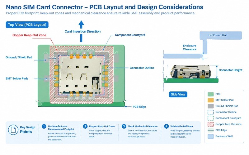
Step 4: Check Mechanical Clearance and Keep-Out Zones
A footprint may be electrically correct but still fail in the assembled product.
Check the connector against:
The PCB edge and card insertion opening.
Enclosure walls and internal ribs.
Nearby components and shields.
Card ejection or hinged-lid movement.
The connector's maximum height and placement tolerance.
Any restricted areas specified in the datasheet.
Distinguish the component courtyard, mechanical clearance, copper keep-out, and soldering area. They serve different purposes and should not be treated as interchangeable.
Engineering note: If the connector is mounted near the PCB edge, review the complete card insertion path and the assembly manufacturer's edge-clearance requirements. Do not assume that one universal clearance value applies to every connector and assembly process.
Step 5: Review Grounding and Signal Routing
After the footprint has been verified, plan the routing for the SIM interface and any card-detection switch.
Keep the routing consistent with the host modem's reference design and electrical requirements. Review trace lengths, return paths, grounding, and the placement of ESD protection devices.
Where appropriate, place ESD protection close to the interface entry point while considering parasitic capacitance, routing topology, and the modem manufacturer's recommendations.
Avoid routing signals through restricted mechanical areas or placing vias where they could interfere with solder pads or assembly.
A connector footprint alone does not guarantee reliable signal integrity or ESD immunity. These properties must be evaluated as part of the complete circuit and product design.
4. SMT Assembly Considerations for Nano SIM Card Connectors
A correctly designed footprint is only one part of a successful SMT process. Solder paste deposition, component placement, reflow, and inspection must all be compatible with the selected connector.
4.1 Solder Paste and Stencil Design
Review the connector's solder pad geometry and the PCB assembly manufacturer's stencil design rules.
Stencil thickness and aperture dimensions should be selected according to the pad layout, component geometry, solder paste, and surrounding components.
For fine-pitch or mechanically sensitive connector designs, the assembly engineer may need to evaluate solder paste volume and aperture geometry to reduce bridging, insufficient solder, or inconsistent joints.
Do not treat a generic stencil thickness or paste coverage percentage as a universal requirement. Establish the process from the connector manufacturer's recommendations and the assembly line's validated process window.
4.2 Component Placement and Orientation
Before assembly, verify the pick-and-place coordinates, component rotation, pin-1 reference, and card insertion direction.
Check that the connector sits flat and aligns with its PCB pads. Confirm that the placement equipment can handle the component without damaging the housing or contact structure.
For connectors with a hinged lid, tray, or moving ejection mechanism, make sure the assembly process does not deform or obstruct the mechanical parts.
4.3 Reflow Soldering Profile
Use the reflow profile recommended for the selected component, solder paste, PCB construction, and assembly process.
Confirm the connector's specified temperature limits and review the applicable moisture-sensitivity or handling requirements where provided.
Do not copy a reflow profile from an unrelated connector simply because both components use SMT mounting.
The actual profile should be validated by the PCB assembly manufacturer using the intended materials and production equipment.
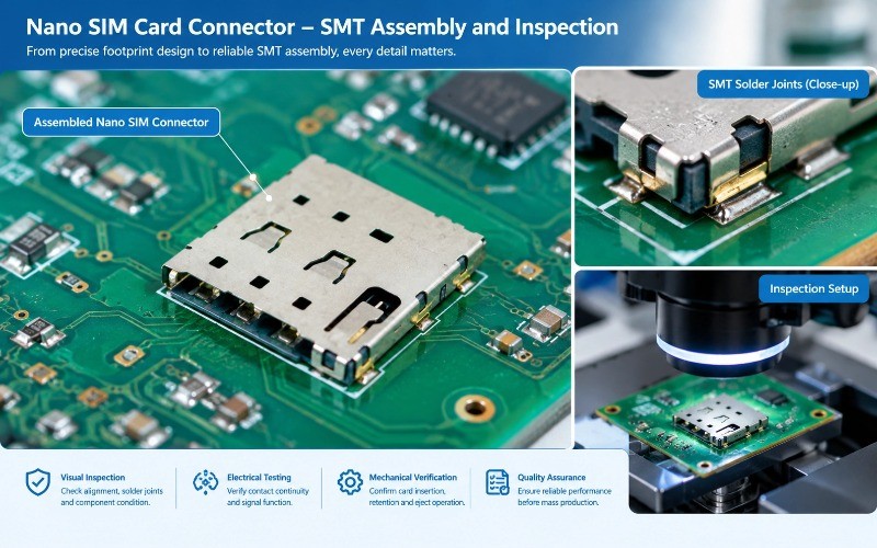
4.4 Inspection After SMT Assembly
A practical inspection plan should include:
Visual inspection of connector alignment and orientation.
Inspection of solder joints for bridging, insufficient solder, or visible defects.
Verification of mechanical mounting and shell connections.
Electrical continuity checks where appropriate.
Card insertion and retention checks.
Functional verification using the host device or test fixture.
Automated optical inspection (AOI) may help identify visible assembly defects, but it cannot replace all electrical and mechanical validation.
5. Common Nano SIM Connector PCB Design Mistakes
Mistake 1: Reusing a Similar Connector's Footprint
Two connectors may accept the same Nano SIM card but have different contact spacing, mounting pads, or mechanical locating features.
Prevention:Verify the footprint against the exact manufacturer part number and current drawing.
Mistake 2: Ignoring Copper Restrictions
Copper, vias, or components placed in a prohibited area can interfere with the connector or compromise the intended assembly.
Prevention:Review all relevant PCB layers and apply the restrictions stated in the manufacturer's drawing.
Mistake 3: Forgetting the Card Insertion Path
The connector may fit the PCB but be inaccessible after the enclosure is assembled.
Prevention:Review the connector, card, PCB, and enclosure together in a 3D mechanical assembly.
Mistake 4: Using an Unverified Third-Party CAD Library
A downloaded footprint may contain incorrect pad sizes, orientation, pin mapping, or outdated dimensions.
Prevention:Compare the library against the official drawing and record the verification result before releasing the design.
Mistake 5: Treating SMT Assembly as a Standard Process
Different connector structures and pad geometries can respond differently to solder paste deposition, placement, and reflow.
Prevention:Confirm the process requirements with the assembly manufacturer and validate the design using production-representative samples.
Mistake 6: Skipping Prototype Validation
A design that passes a CAD review may still experience card retention problems, solder defects, or enclosure interference.
Prevention:Assemble prototypes and verify both mechanical fit and electrical function before mass production.
6. Nano SIM Card Connector PCB Design Verification Checklist
Use this checklist before releasing the PCB for fabrication and assembly.
Footprint Verification
Exact manufacturer and part number confirmed.
Latest mechanical drawing and datasheet reviewed.
Pad dimensions, spacing, and numbering verified.
Connector orientation checked against the schematic.
Mounting pads and locating features reviewed.
Copper restrictions and keep-out zones applied.
Component height and enclosure clearance checked.
Footprint library revision documented.
SMT Process Review
Solder paste and stencil design reviewed.
Pick-and-place coordinates and rotation checked.
Reflow requirements confirmed.
Inspection criteria defined.
Assembly process reviewed with the PCB manufacturer.
Prototype Validation
Connector alignment and solder joints inspected.
Card insertion, retention, and removal verified.
Electrical contact and card-detection functions checked where applicable.
Host device recognizes and communicates with the SIM.
Mechanical and environmental tests defined for the intended application.
Design changes and verification results documented.
The checklist should be adapted to the connector datasheet, application requirements, and manufacturing process. It is not a substitute for formal product qualification.
7. How MoarConn Supports Nano SIM Connector PCB Integration
Selecting a Nano SIM Card Connector is not only a component purchasing decision. It also involves mechanical integration, PCB design, assembly compatibility, and product validation.
Moarconn specializes in card connector research and development, manufacturing, sales, and service, with a product portfolio that includes Nano SIM, SIM, SD, Micro SD, and smart-card connectors.
For engineers developing compact or connected devices, Moarconn supports the connector development process through product selection, mechanical design coordination, tooling, assembly, and customer-specific engineering support.
Depending on the selected model and project requirements, engineers can evaluate different connector structures, mounting options, profile heights, and mechanical configurations.
Engineering Support from Design to Production
Moarconn's engineering collaboration can help project teams review:
Connector dimensions and available installation space.
PCB integration and mechanical clearance.
Card insertion and retention requirements.
Product-specific connector configurations.
Prototype evaluation and production preparation.
For custom connector projects, early coordination between the connector supplier, PCB designer, and assembly manufacturer can help identify footprint or mechanical conflicts before tooling or mass production.
Explore the MoarConn Nano SIM Card Connector portfolio or visit Moarconn to discuss your project requirements.
Need help selecting a Nano SIM Card Connector for your PCB?Share your required connector height, mounting method, card insertion mechanism, available PCB space, and expected application conditions with the MoarConn team. These details can help narrow the selection and establish the next steps for technical review.
8. Frequently Asked Questions
What is a Nano SIM Card Connector PCB footprint?
A Nano SIM Card Connector PCB footprint defines the PCB pads, component outline, and relevant mounting information required to install the connector. The exact footprint depends on the selected part number. Moarconn recommends verifying the manufacturer's mechanical drawing and recommended land pattern before PCB release.
Where can I download a Nano SIM connector PCB footprint?
Check the connector manufacturer's official product page and datasheet for recommended PCB layouts, CAD files, or footprint downloads. Some component libraries also provide CAD symbols and footprints, but these should be verified against the official drawing. Moarconn can help engineers review connector options and PCB integration requirements for suitable products.
Can I use the same PCB footprint for different Nano SIM connectors?
Not without verification. Connectors that support the same card format may differ in pad geometry, pin numbering, mounting structure, height, and mechanical clearance. Moarconn advises checking the exact part number and comparing the proposed footprint with its current technical drawing.
What should I check before SMT assembly?
Verify the footprint, pad geometry, connector orientation, pick-and-place coordinates, solder paste and stencil requirements, reflow profile, and inspection criteria. The process should be validated for the actual connector and PCB assembly conditions. Moarconn can work with project teams to review connector-specific integration requirements.
How can I prevent Nano SIM connector soldering defects?
Start with the correct recommended land pattern, follow the assembly manufacturer's process rules, and inspect the assembled joints. Potential defects include solder bridging, insufficient solder, misalignment, and damaged mechanical features. The appropriate corrective action depends on the observed defect and the validated assembly process.
What information should I provide when requesting a Nano SIM connector?
Provide the card format, maximum connector height, mounting method, insertion mechanism, available PCB area, contact or card-detection requirements, operating environment, target quantity, and expected schedule. A PCB layout or enclosure drawing can also help the engineering team assess mechanical fit.
Conclusion
A reliable Nano SIM Card Connector PCB design begins with the correct component footprint and continues through mechanical review, SMT process planning, and prototype validation.
By verifying the official land pattern, respecting keep-out areas, checking the complete card insertion path, and validating the assembled product, engineers can reduce avoidable design errors before mass production.
Moarconn supports Nano SIM and other card connector requirements through product selection, connector development, manufacturing, and engineering collaboration.