Optimizing High-Speed Data Integrity in Micro SD Connector Designs
- Share
- publisher
- MOARCONN
- Issue Time
- Jun 20,2025
Summary
Why Data Integrity Matters in High-Speed Designs ?
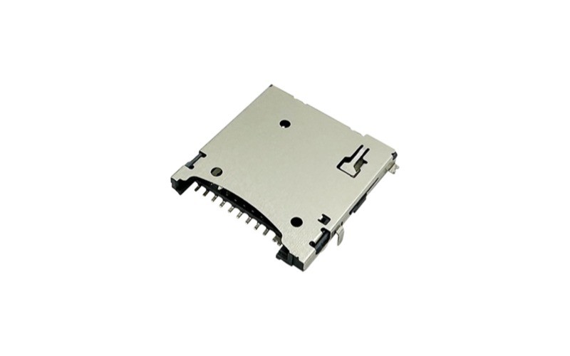
Why Data Integrity Matters in High-Speed Designs
Understanding Signal Integrity Challenges

Design Techniques for High-Speed Micro SD Connectors
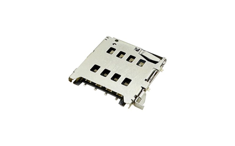
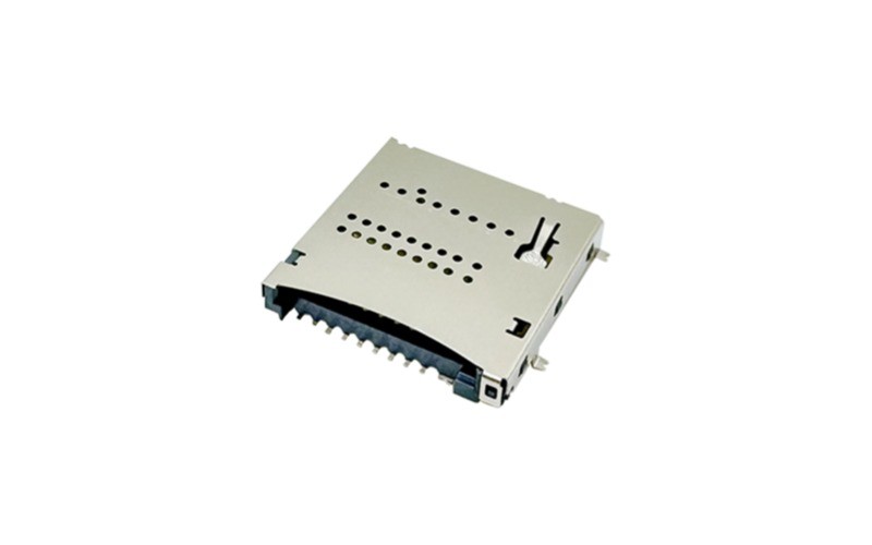
Failure Map: What Actually Breaks at 104MB/s
Signal integrity work goes faster when you stop treating "bad SI" as one problem. At UHS-I speeds the failure modes are distinct, they have different root causes, and they show up at different points in the test cycle. The table below maps the four symptoms engineers report most often to the physical mechanism behind them.
| Symptom | Physical mechanism | Where it originates | First thing to change |
|---|---|---|---|
| Card drops to a slower speed mode | Return loss from an impedance discontinuity | Pad-to-trace transition, via stub under the connector | Shorten the stub, re-tune the pad geometry |
| Intermittent CRC errors under write load | Crosstalk between CLK and DAT lines | Parallel routing under the shell, missing ground between pairs | Increase spacing or add a ground trace |
| Throughput falls off after warm-up | Contact resistance drift with temperature | Plating thickness, wipe length, terminal force | Specify ≥0.025µm gold, check force curve |
| Fails EMC pre-scan but works on the bench | Common-mode current on the shield | Shell grounding points, cable or slot aperture | Stitch the shell to ground at multiple points |
The pattern is worth remembering: three of the four are layout decisions made before the connector is chosen, and one — contact resistance drift — is the only one the connector manufacturer fully controls. That is why the supplier conversation should be about plating, force and coplanarity, while the layout conversation stays in-house.
Impedance Targets and Stack-Up for SDIO Traces
The micro SD interface is single-ended, not differential, so the target is 50Ω single-ended on every signal line with a solid reference plane directly beneath it. On a four-layer board with 0.1mm prepreg this usually lands at a 0.2mm trace width; on a six-layer board with a closer reference plane the trace gets narrower. Do not copy a width from another project — the number that matters is the one your fabricator's stack-up produces.
CLK is the net that decides whether the link trains at SDR104 or falls back. Treat it as the critical net: route it on a single layer from pad to controller, keep it at least three trace widths from any DAT line, and never let it run parallel to a switching regulator output. DAT0 to DAT3 should be length-matched to within a few millimetres at default speed and tighter as the clock rises; CMD is less sensitive but should still avoid layer changes.
Two layout habits cost more than they save. The first is routing under the connector body to gain space — the shell is a metal can, and a trace that runs beneath it sees a changing reference and a resonator. The second is necking the trace down to fit between pads without adjusting the reference plane; a 0.15mm neck in a 0.2mm line is a visible discontinuity at 200MHz and shows up as return loss on a TDR trace.
Grounding and Shielding: Where the Return Path Actually Goes
Every high-speed trace needs a return current, and at 100MB/s that current does not take the path of least resistance — it takes the path of least inductance, which is directly under the trace. If the ground plane under the connector is slotted by a via field or a power island, the return current detours, the loop area grows, and both crosstalk and emissions rise together.
Three rules cover most cases. Keep an uninterrupted ground plane on the layer directly below the SDIO traces, with no slots or plane splits crossing under the connector footprint. Ground the metal shell at multiple points — at minimum both ends, ideally at every mounting tab — because a shell grounded at one corner behaves like an antenna. And place stitching vias along the edge of the connector footprint at intervals shorter than a tenth of the wavelength at your highest frequency, which for 200MHz signalling means roughly every 3mm to 5mm.
The shell itself is part of the design, not packaging. A well-grounded shell reduces radiated emissions from the slot aperture and improves crosstalk rejection between adjacent contacts. MOARCONN's high-speed micro SD series uses an optimised shell shielding geometry for exactly this reason, and the effect is measurable in a pre-scan even when the PCB is unchanged.
Contact Resistance Stability Across Temperature and Vibration
A connector that measures 20mΩ on the bench and 45mΩ after a thermal cycle has not failed a specification — it has revealed that the specification was measured at the wrong condition. MOARCONN rates contact resistance at 30mΩ or less with terminals plated to at least 0.025µm of gold over nickel on phosphor bronze, and holds that figure from -45°C to 80°C. Ask any supplier whether the resistance figure is dry-circuit, at rated current, or after cycling; the three numbers can differ by a factor of two.
Thermal cycling works on the contact in two ways. Differential expansion between the terminal and the housing changes the normal force, so a design with marginal force loses contact pressure at the cold end. And every cycle moves the wipe point slightly, so a thin plating wears through to the nickel barrier sooner than a cycle count on a datasheet would suggest. This is why plating thickness and contact force belong in the same conversation.
Vibration is the other half. For automotive telematics and transport recorders, ask for ISO 16750-3 evidence rather than a generic "vibration tested" claim; the profile matters more than the pass mark. MOARCONN manufactures under ISO 9001, ISO 14001 and IATF 16949, and has ISO 16750-3 vibration data available for automotive programs.
How to Prove It Before You Build 10,000 Units
Signal integrity problems are cheap to find on a first article and expensive to find in the field. A short verification sequence that catches most of them:
- TDR on the bare board. Measure impedance along the CLK and DAT traces with the connector fitted. Look for a step at the pad, not just an average number.
- Eye diagram at the highest speed mode you claim. Run it at the temperature extreme, not at room temperature only — dielectric loss rises with heat and the margin you measured at 25°C is not the margin you ship.
- Write-load soak with CRC counters. Read-only tests hide crosstalk; sustained writes are where retries appear.
- Contact resistance before and after 500 thermal cycles, measured at the same current both times.
- EMC pre-scan with the final enclosure, because the slot aperture is part of the antenna.
From the supplier side, ask for four documents and you will avoid most surprises: the dimensional drawing with coplanarity tolerance, the plating specification with thickness and under-plate, the force curve across the rated life, and the material declaration. MOARCONN provides these as standard with samples, retains samples for 3 years for traceability, and supports custom pin layouts on a 25-day development cycle with 0 MOQ and 7-day sampling.
High-Speed Micro SD Connector FAQ
Does the connector itself affect throughput, or is it all PCB layout?
Both, but in different frequency bands. Below about 50MHz the connector is close to transparent and layout dominates. At UHS-I speeds the contact geometry, plating quality and shell grounding start to matter, because contact resistance variation and the pad-to-terminal transition both create the discontinuities that produce return loss. A good layout cannot rescue a connector with unstable contact resistance, and a good connector cannot rescue a 5mm stub.
Can I use the same footprint for UHS-I and UHS-II?
No. UHS-II adds a second row of contacts and needs a controlled-impedance differential pair routed to it, which changes both the pad geometry and the layer assignment. If there is any chance the product will move to UHS-II or SD Express later, decide that before the first layout — retrofitting a second row onto an existing footprint is a respin, not a revision.
What plating thickness do I need for a high-speed socket?
At least 0.025µm of gold over nickel is the practical floor for a part rated to 10,000 cycles at 30mΩ or less. Plating does not change the high-frequency behaviour much directly, but it controls how stable the contact resistance stays after thousands of insertions and thermal cycles, which is what causes the slow throughput degradation engineers usually blame on firmware.
How do I test signal integrity without owning a VNA?
Start with the eye diagram from your controller's built-in tuning tool and a write-load soak with CRC error counters — those two catch most real failures and need no lab equipment. Use a contract lab for TDR and EMC pre-scan at the first article. If a supplier cannot provide a force curve and a plating report, the measurement problem is upstream of your test plan.
MOARCONN's High-Speed Micro SD Connector Solutions
Real-World Application Example
Conclusion
MOARCONN Quality Anchors
Every MOARCONN card socket connector is validated to 10,000 mating cycles (tested to GB/T 5095.7-1997; over 2× the 3,000–5,000 cycles common in the industry), operates from -45°C to 80°C, and ships with contact resistance ≤30mΩ thanks to ≥0.025µm gold-plated phosphor-bronze terminals. IATF 16949 certified production supports 0 MOQ orders with 7-day sampling and a 25-day development cycle — backed by in-house mold, stamping and injection molding factories and 32 granted patents.